SC/MP Elektor Emulator V0.9 Background Info
This Webpage is dedicated to the very first CPU I ever used and with which I build two homebrew systems. Over the last couple of years I've been working (hap-hazardly) on an emulator for this CPU. As of now I think the emulator functions well enough to put it up for those users that want to try it. However I will not make any guaranties to it's reliable functioning yet. The program must considered to be in the alpha-test phase.
| SC/MP Emulator Downloads | ||||
| Download Elektor Emulator | The Emulator was written in Visual Basic 6.0 and needs the required runtime-files which is also available | |||
| Download NIBL Emulator | The NIBL emulator was send to me by Henri Mason. He wrote this emulator in Microsoft Visual C++ and integrated the NIBL ROMS. This means that it runs the NIBL very tiny BASIC. When I get to it and I can find my old National Semiconductor documentation I will scan some more info on the NIBL stuff and make it available here | |||
Preface
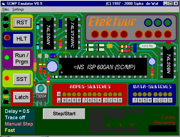
In this documentation you will find technical background information on the SC/MP-CPU (say SCAMP) from National Semiconductor. This is additional information for those who want to work with the SC/MP Emulator. We will cover some history, hardware info, PIN-OUT-description, CPU-register-set, addressing-modes, the instruction-set and some sample programs. Below is a screendump of the emulator.
National Semiconductor introduced the SC/MP-In April 1976, almost 25 years to this day. It was intended for small industrial controllers, appliances and entertainment devices. The acronym SC/MP stand for Small Cost-effective Micro Processor. It needed few external components by the standards of those days and was easy to program. Nowadays one would use small embedded controllers like PICs or 804X/805X-chips for the same purposes.
In The Netherlands the SC/MP was frequently used in climate control applications used in the greenhouses of The Westland region near Delft and The Hague. In 1977 Elektor Magazine devoted a substantial number of issues to the SC/MP so the reader could get first-hand knowledge of a new phenomenon; "The Microprocessor". The Elektor design came in two versions. The first design is as emulated by me (although my emulator has many features not covered in the original hardware). The second design featured a hexadecimal keyboard and 8x 7-segments-led display. And had a true monitor program in ROM, cassette interface and the option to connect a VDU.
Eventally I build both designs, but the first version was my virgin experience with computer hardware and it stuck. So from a nostalgic point of view I found it worth while to devote some time over the last couple of years to write the emulator. It is written in Visual Basic 6.0 and the reader is free to examine and fiddle with the source-code.
The SC/MP microprocessor blockdiagram & pinouts
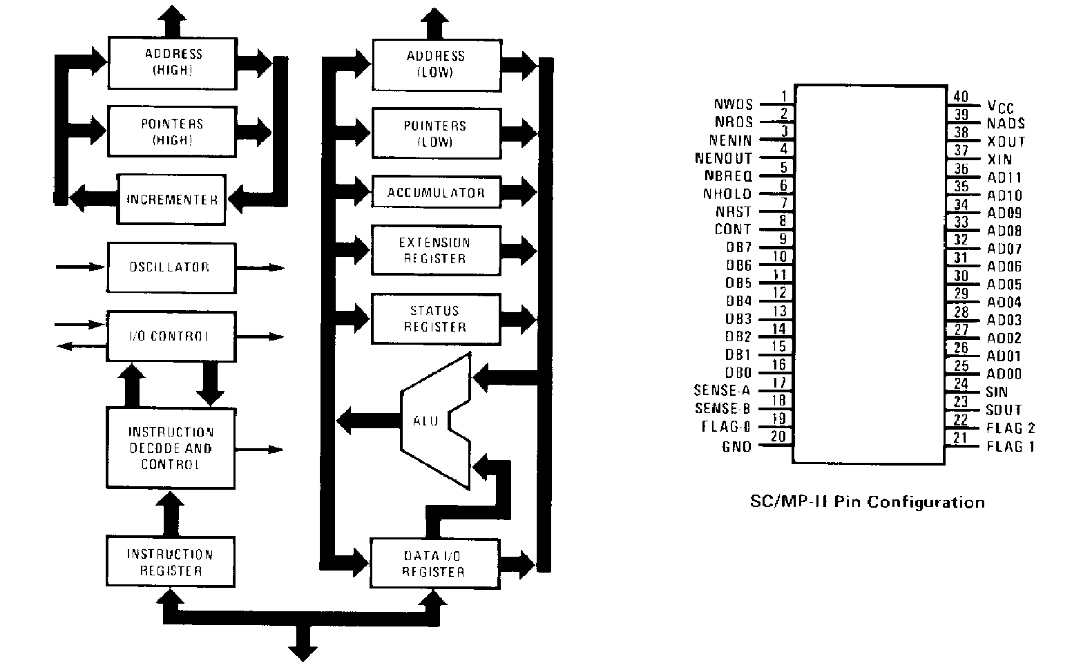
In the right part of the above image you can see that the SC/MP has 40 pinouts. At the left a block diagram of the SC/MP-Is shown.
The SC/MP has a rather mini-computerlike architecture and can address a total of 65536 bytes memory locations by means of a 16-bit address-bus. Because only 12 of these address lines are directly connected to pinouts, simple applications could disregard the 4 MSB-address lines that were multiplexed on the data bus during the NADS-signal. This would result in a design with a lower chipcount. The 65k memory locations are divided in 16x 4096-bytes called pages. Only a limited number of memory reference instructions can cross a page boundary, so the SC/MP was often used with rather limited amount of memory.
My most complicated design featured 9Kbytes of RAM and Tiny-basic in 4K ROM. It was hooked up to a VDU, an ASR33 Teletype and had a cassette-interface for storage. Nevertheless in 1978 I was the first at my school to deliver notes and projects in a typed form and had some crude textprocessing software on this SC/MP-system to pull it off.
The SC/MP-chip was developed in two versions. The SC/MP-I in P-MOS technology had a positive power supply of 5 Volts and a negative supply of 7 Volts. Later National Semiconductor introduced the SC/MP-II that was made in N-MOS technology and had a single 5 Volt power need. Three of the signals on the SC/MP-II were logically reversed (i.e. BREQ became NBREQ) so the SC/MP-II is not 100% pin-compatible with the SC/MP-I. The SC/MP-II could be clocked with a four times higher frequency (4 MHZ) but this was internally divided by two, so the SC/MP-II was effectively 2x faster than the SC/MP-I. So back then kludging a SC/MP-II in your SC/MP-I system certainly was an option, double speed .. Wow!
Design Basics
In the diagram below a simple SC/MP system is shown. Nowadays this logic could be implemented on one chip a 1000 times over, and you would still have space to add additional features. (grin)
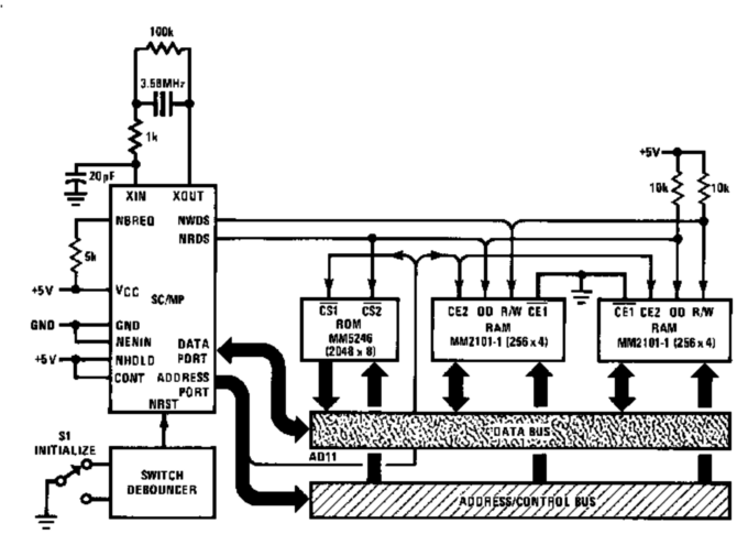
 The SC/MP is connected by means of an addressbus and a databus to a ROM and 2 RAM chips. The program in ROM first has to be developed in a development-system. Possible variations on this theme could be the addition of a 7-segment LED-display and a keyboard to facilitate a user-interface. In a controller application one might want to add a few solid-state-relays to switch a large load. The SC/MP has 3 direct outputs (FLAGS) that could be used for this. It even has a rudimentary serial I/O capability on chip that could be turned in to a very crude Analog-to-Digital-Converter (ADC). Nice for measuring temperature or other analog data that doesn't require high speed sampling.
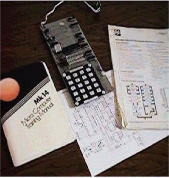
Another variation on the above scheme that gathered some fame was the MK14, developed by Science of Cambridge Ltd, which was a company of Sir Clive Sinclair. (see picture). There is also an emulator for the MK14 by Paul Robson (available in the file-section of my website:
http:/files/Emulator/).The Elektor design on which my emulator is based did not require a monitor-program in ROM. By fiddling with the address- and data switches you could dump (latch) binary data straight into the 256-bytes of RAM and then run the program. Just like an old minicomputer or an Altair. My emulator has the added features of loading and dumping memory image or loading a small pseudo-assembly program into RAM, but on the real thing you had to fiddle with dip-switches each time you wanted to work with it, and no way to save your work. (arrrhhh!!). Needless to say I got rather proficient at thinking in binary and hexadecimal.
OK, The SC/MP was not exactly a powerfull microprocessor as compared with contemporary chips like the P4 and the Athlon, but at the time it was affordable (~ U$25,- ) in relation to CPUs like the 8080 for which you would still had to fork out U$100 and which also required a lot of additional chips to make a basic system.
The SC/MP only an instructionset of 46 basic instructions and was rather easy to program at the binary level. Remember you needed to hand-assemble all programs on a 8080 that would have been a major task for a startup like me! All in all it was a nice learning experience.
Multi-processor support
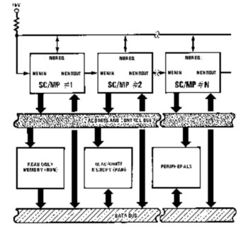
There is one feature of the SC/MP that is not widely known: It has build-in multi-processor capabilities. You can actually connect up to three SC/MP chips in one simple system and let them run on the same address- and databus cooperating in the execution of their task. The SC/MP contains logic for a BUS-request and BUS-grant system that enables 3 SC/MPs to access the busses in a synchronised daisy-chain fashion. Propably more than three SC/MP could be connected in this way but this would saturate the use of the bus and outweigh the advantage of using additional chips. Nevertheless multiprocessing build-in was quite a advanced feature in 1976.
The multi-processor arbitration logic can also be abused to implement a DMA (Direct Memory Access) transaction but save the arbitration logic all DMA-logic must be implemented external to the CPU with other of the shelf logic. Some 8080 support chips can be used in conjunction with the SC/MP.
Pinouts
In order for the SC/MP to easily communicate with the outside world the SC/MP has three outputlines directly connected to pinouts (Flags 0,1 & 2) and two inputlines (Sens A & B). Sense A can also be used as an interupt request line in the interupt enable flag in the status-register is set. Furthermore it has a build-in serial I/O capability by means of the SIN and SOUT lines that can shift data in and out of the extension-register. Al lot of applications used one of the flags and one of the sense-lines (Sense B) as an additional serial interface under program control. In this way I was later able to hook up a VDU (simple terminal) and a cassette-interface. The VDU could even be switched for the ASR33 teletype to allow for hardcopy. Remember that all these facilities came directly from the SC/MP chip, save for some buffering devices. The SC/MP signals are TTL-compatible and could drive a load of 2 to 4 74LSXX devices without buffering. Where speed was not a great factor CMOS-logic could be used to diminish loaddriving needs. The chip was rather rugged and could sustain a lot of abuse, altough I did mange to blow up a flag-output line once.
The table below describes the various SC/MP signals and pinouts.
(A preceding "N" in the signal mnemonic signifies a negative active signal.)
|
Mnemonic |
Functional Name |
Description |
|
NRST |
Reset Input |
Set high for normal operation. When set low, aborts in-process operations. When returned high, internal control circuit zeroes all programmer-accessible registers; then, first instruction is fetched from memory location &H0001 |
|
CONT |
Continue Input |
When set high, enables normal execution of program stored in external memory. When set low, SC/MP operation is suspended (after completion of current instruction) without loss of internal status |
|
NBREQ * |
Bus Request In/Output |
Associated with SC/MP-Internal allocation logic for system bus. Can be used as bus request output or bus busy input. Requires external load resistor to Vcc |
|
NENIN * |
Enable Input |
Associated with SC/MP-Internal location logic for system bus. When set low, SC/MP-Is granted access to system busses. When set high, places system busses in high-impedance (TRI-STATE) mode. |
|
NENOUT * |
Enable Output |
Associated with SC/MP-Internal allocation logic for system bus. Set low when NENIN is low and SC/MP-Is not using system busses (NBREQ-high. Set high at all other times.) |
|
NADS |
Address Strobe Output |
Active-low strobe. While low, indicates that valid address and status output are present on system busses. |
|
NRDS |
Read Strobe Output |
Active-low strobe. On trailing edge, data are input to SC/MP from 8-bit bi-directional data bus. High-impedance (TRI-STATE) output when input/output cycle is not in progress. |
|
NWDS |
Write Strobe Output |
Active-low strobe. While low, indicates that valid output data are present on 8-bit bi-directional data bus. High-impedance (TRI-STATE) output when input/output cycle is not in progress. |
|
NHOLD |
Input/Output Cycle Extend Input |
When set low prior to trailing edge of NRDS or NWDS strobe, stretches strobe to extend input/output cycle; that is, strobe is held low until NHOLD signal is returned high. (for slow memory) |
|
SENSE A |
Sense/Interrupt Request Input |
Serves as interrupt request input when SC/MP-Internal IE (Interrupt Enable) flag is set. When IE flag is reset, serves as user-designated sense condition input. Sense condition testing is effected by copying status register to accumulator. |
|
SENSE B |
Sense Input |
User-designated sense-condition input. Sense-condition testing is effected by copying status register to accumulator. |
|
SIN |
Serial Input to E register |
Under software control, data on this line are right-shifted into E register by execution of SIO instruction. |
|
SOUT |
Serial Output from E register |
Under software control, data are right-shifted onto this line from E register by execution of SIO instruction. Each data bit remains latched until execution of next SIO instruction. |
|
Mnemonic |
Functional Name |
Description |
|
|
FLAGS 0,1,2 |
Flags Outputs |
User-designated general-purpose flag outputs of status register. Under program control, flags can be set and reset by copying accumulator to statusregister. |
|
|
AD00-AD11 |
Address bits 00 through 11 |
Twelve (TRI-STATE) address output lines. SC/MP outputs 12 least significant address bits on this bus when NADS strobe is low. Address bits are then held valid until trailing edge of read (NRDS) or write (NWDS) strobes. After trailing edge of NRDS or NWDS strobe, bus is set to high (TRI-STATE) mode until next NADS strobe. |
|
|
Databus |
Output (at NADS Time) |
During NADS time the four most significant bits of the addressbus are active at the outputs. Also some other special signals are available at the remaining database pinouts. |
|
|
DB0 |
Address Bit 12 |
Fourth most significant bit of 16-bit address |
|
|
DB1 |
Address Bit 13 |
Third most significant bit of 16-bit address |
|
|
DB2 |
Address Bit 14 |
Second most significant bit of 16-bit address |
|
|
DB3 |
Address Bit 15 |
Most significant bit of 16-bit address |
|
|
DB4 |
R-Flag |
When high, data input cycle is starting; when low, data output cycle is starting |
|
|
DB5 |
I-Flag |
When high, first byte of instruction is being fetched |
|
|
DB6 |
D-Flag |
When high, indicates delay cycle is started; that is, second byte of DLY instructions being fetched |
|
|
DB7 |
H-Flag |
When high, indicates that HALT instruction has been executed. (In some system configurations, the H-Flag output is latched and, in conjunction with the CONTinue input, provides a programmed halt). |
|
|
Databus |
Standard Output |
||
|
DB0-DB7 |
Databus input/output |
During the assertion of NWDS or NRDS data is written to or read from external devices. Except for NADS-time, at all other times the databus is floated in (TRI-STATE) modus |
|
|
Vcc |
Plus 5 volts |
Power lead |
|
|
GND * |
Ground (0 Volts) |
Power ground lead SC/MP-II (P-MOS) |
|
|
Vgg |
Minus 7 Volts |
Power negative lead SC/MP-I (N-MOS) |
|
|
XIN/ XOUT |
Clock Crystal inputs |
A quarts crystal between these leads will determine the clock-frequency of the SC/MP CPU. The SC/MP-II has an internal divide stage so its clock-frequency is effectively halved. |
|
|
TRI-STATE |
Special TTL-bus compatible output |
In normal circumstances logical information can only travel on a system bus from an output-line to an input-line. By means of the TRI-STATE function the output pin can effectively be isolated from the bus and hence another pin on the bus can now take the role of the TTL-output (TTL = Transistor-Transistor-Logic) |
|
|
* |
SC/MP-II |
All pinouts marked with an asterisk denotes the fact that these pinouts changed with the introduction of the SC/MP-II and that they are not exactly pincompatible with the SC/MP-I. Here the SC/MP-II nomenclature is used except for Vgg |
|
SC/MP-Instruction format
The SC/MP executes either 1- or 2-byte instructions. The first byte is called the OPCODE the optional second byte is the OPERAND. Whenever the most significant byte of the OPCODE is set high it will signify a 2-byte instruction. In that case the programcounter (P0) is automatically incremented and the second byte is feched.
|
bits |
7 |
6543210 |
76543210 |
|
Opcode |
Operand |
||
|
1 Byte instruction |
0 |
XXXXXXX |
Nvt |
|
2 Byte instruction |
1 |
YYYYYYY |
ZZZZZZZZ |
Most 2-byte instructions are memory-reference instruction that will access memory external to the CPU. With the exception of the ILD and the DLD instruction, upon calculating the effective address based on the opcode and the operand the SC/MP will initiate a single byte read or write memory access. The ILD and the DLD however instruction will do a read-modify-write instruction. During these two cycles the bus will be locked for any other (external) operation. So DMA-circuitry will have to know about this
The Programmable SC/MP registers:
|
15 |
14 |
13 |
12 |
11 |
10 |
9 |
8 |
7 |
6 |
5 |
4 |
3 |
2 |
1 |
0 |
<-bits |
|
8 Bits |
Msb |
Lsb |
Accu |
|||||||||||||
|
Msb |
Lsb |
Extension |
||||||||||||||
|
CY |
OV |
SB |
SA |
IE |
F2 |
F1 |
F0 |
Status |
||||||||
|
16 Bits |
||||||||||||||||
|
Msb |
lsb |
P0 (PC) |
||||||||||||||
|
Msb |
lsb |
P1 |
||||||||||||||
|
Msb |
lsb |
P2 |
||||||||||||||
|
Msb |
lsb |
P3 |
||||||||||||||
Accu
This is a reasonably standard accumulator-register that contains the result of the most operations and usually holds one of the source operands. Like in the next example:
LDI 08 (Accu=8)
ADI 01 (Accu=8+1 è 9)
Extension
The extensionregister is a bit of a multi purpose story. It can be used to hold secondary operands to the extension instructions, it can be used to temporarily save the accu and it can be used as an 8-bit index register to facilitate relative indirect addressing. Whenever the 2nd-byte operand of a memory-reference instruction (called the displacement) holds a value of &H80 the content of the extension register is taken as the displacement instead of the 2nd-byte operand.
Furthermore the extension register is also used for the build-in serial I/O capability of the SC/MP. The MSB of the extension register is connected to the SIN-input and the LSB is connected to the SOUT-output line. A number of timed serial shift instructions can now be issued to input and output serial data (if desired simultaneously).
Status
The status register contains a number of rather standard flags like the carrylink-flag and the overflow-flag and the interupt-enable-flag. However, the carry and overflow flags are not directly tested by branch-instructions. They must be copied to the accu first (CAS-instruction) and their state must be ascertained with bitwise logical instructions. Branch-testing is only done on the state of the accu-register.
The other status bits are:
- Flag F0, F1 & F2 that are connected to the flag pinout for output.
- Sense SA & SB that are connected to the sense input pinouts.
When interupts are enabled by setting the interupt enable flag the Sense A pinout will double as a interupt input. Upon an interupt the SC/MP will automatically execute a XPPC3 instruction. Pointer-register P3 will have to point to an interupt service-routine. XPPC3 will exchange the content of the PC with P3 when the interupt triggers. No CPU-registers are saved when an interupt occurs, the interupt service-routine must take care of this.
The Pointer Registers P0-P3
The Pointer-registers P1-P3 are used as datapointer, stackpointer and subroutine/ interupt service pointer respectively.
Pointerregister P0 is used as the Programcounter. The main difference with a normal programcounter is the fact that the SC/MP PC is incremented prior to fetching a new instruction, so the program always continues the next instruction at PC+1.
Another feature of all pointer-registers is the fact that whenever a pointer-register is incremented by a auto-indexed-addressing-mode instruction or an effective address is calculated that crosses a page boundary (i.e. 0FFF->1000) the boundary cross is not taken but the resulting Px-content or effective address folds back to the beginning of the page (0FFF->0000). Only by loading an absolute address into the pointer-register can a page-boundary be crossed!
Apart for the special role of the program-counter an the interupt-service-routine pointer (P3) all pointer-registers function identical. National Semiconductor the following pointer-register roles as a rule of thumb.
P1 = Data of I/O Pointer (see: Indexed Addressing)
P2 = Stackpointer (see: Auto Indexed Addressing)
P3 = Subroutine/interrupt Pointer (see: Subroutine explanation)
Now you are not exactly bound to this role distribution it does make sense to abide by it. Especially with regard to the role of P3 that serves as the pointer to subroutines or the interupt-service-routine.
The XPPC instruction can exchange the content of the PC with any of the other pointer-registers so any Px can service a subroutine but only P3 can service a service-routine for an interupt, because the XPPC3 instruction is generated automatically whenever an interupt is received.
The following code exemplifies the SC/MP subroutine method:
|
@0000 |
ORG=0000 |
||
|
NOP |
No operation |
||
|
LDI |
08 |
Load &H08 in Accu |
|
|
XPAH3 |
|||
|
LDI |
00 |
Load &H00 in Accu |
|
|
XPAL3 |
Exchange Accu with high byte of P3 |
||
|
(P3 now contains the subroutineaddress1) |
|||
|
XPPC3 |
Call Subroutine |
||
|
@0800 |
ORG=0800 |
||
|
NOP |
No operation (makes it easy to determine start of routine) |
||
|
:Subroutine |
|||
|
XAE |
Exchange Accu with Extension to save the content of the ACCU |
||
|
Subroutine code goes here |
|||
|
XAE |
Again exchange Accu with extension to reclaim old Accu content |
||
|
XPPC3 |
Return from subroutine |
||
|
JMP |
:Subroutine |
||
|
(This last JUMP is typical for the SC/MP-subroutine execution method, because upon the XPPC3 that returns from the subroutine P3 will now point to this jump instruction that itself points back to the start of the subroutine enabling subsequent subroutine calls. The same goes for an interupt-service-routine .) |
|||
Addressing Modi
All memory reference instructions make use of addressing-modes to calculate the effective address of the memory reference. This could be to access the content of a memory location or to determine the targetaddress of a branch- or jumpinstruct ion.
The SC/MP features the following addressingmodes:
PC Relative/Pointer-register Indexed Addressing
The 2nd byte of an instruction is taken as a displacement in 2s-complement fashion and added to the current content of the designated pointer register to calculate the effective address. When the PC (P0) is used as the designated pointer-register we call this PC-relative mode. A 2s-complement 8-bit value can contain any value from 127dec to + 127dec ( &H81 to &H7F in hexadecimal notation).
In the case of a PC-relative Jump (branch) one should take into consideration the the programcounter will be incremented by 1, prior to the next opcode fetch.
|
@0000 |
ORG=0000 |
||||
|
0000 |
08 |
NOP |
|||
|
0001 |
C0 |
LD |
P0(+4) |
||
|
0002 |
04 |
||||
|
(Load a value YY from memory, where the effective address is equal to the content of the PC (=0002) upon completion of the fetch of the second part of the instruction + 4 (EA=0002+0004=0006)) |
|||||
|
0003 |
90 |
JMP |
:Label |
||
|
0004 |
06 |
||||
|
(Now jump over 6 bytes (upon loading the jumpinstruction PC=0004) to continue the remaining program. (EA=0004+0006=>000A) However the PC will increment by 1 prior to fetching the next opcode so the program should continue at 000B) |
|||||
|
0005 |
08 |
NOP |
|||
|
:VALUE-X |
0006 |
YY |
The load instruction found its target here |
||
|
0007 |
08 |
NOP |
|||
|
0008 |
08 |
NOP |
|||
|
0009 |
08 |
NOP |
|||
|
000A |
08 |
NOP |
|||
|
:Label |
000B |
C0 |
LDI |
XX |
Remainder of the program |
|
XX |
|||||
Now this is not good programming practice but it suffices to show us how PC-relative and indexed addressing operate. Both examples used positive displacements and their target lays ahead of the current PC-value but you could just as easily have used a negative value. For a jump instruction this would lead to a program loop. This is shown in the next example:
|
@0200 |
ORG=0200 |
||||
|
0200 |
08 |
NOP |
|||
|
:Loop |
0201 |
C1 |
ST |
P1(+0) |
Store Accu to LEDs |
|
0202 |
00 |
||||
|
0203 |
F4 |
ADI |
01 |
Add immediate 1 to Accu |
|
|
0204 |
01 |
||||
|
0205 |
9C |
JNZ |
:Loop |
Jump Back if Accu is not equal to 0 |
|
|
0206 |
FA |
(negative displacement for jump) |
|||
|
0207 |
C4 |
LDI |
XX |
Remainder of Program |
|
|
0208 |
XX |
||||
|
0209 |
Indirect Addressing
In SC/MP literature indirect addressing is regarded as a special case of PC-relative and indexed addressing. In the event that the second byte of an memory reference instruction contains &H80 as a displacement value It is not taken as a negative displacement of 128dec But the content of the extension register is used as the 2s-complement displacement to calculate the effective address.
Immediate Addressing
The second value of the instruction in a memory reference instruction is immediately used as source data for the instruction. No further address calculation is required.
Auto Indexed Addressing
This addressing mode is a bit like Indexed addressing but this time the pointer-register itself is modified by the displacement. This in a pre-decrement and post-increment fashion.
- In the case of a negative displacement the pointer-register is replaced with the effective address and then the memory access is executed.
- In the case of a positive displacement the memory access is executed with the current value of the designated pointer-register, prior to replacing Px with the new modified calculated EA-value.
In this way we can used P1, P2 or P3 as a LIFO stackpointer. This addressing mode has no relevance in conjunction with the PC so there is no PC-relative variation on this theme. The next program sample shows us how this works
|
@0800 |
|||
|
NOP |
No operation |
||
|
:Subroutine |
ST |
@P2(-1) |
|
|
(Push Accu on stack (Pointer reg will be pre-decremented by 1 and the content Accu will be written to EA) |
|||
|
Here goes the main subroutine code |
|||
|
LD |
@P2(+1) |
||
|
(Pop Stack (the post-increment feature will pop the top of stack prior to storing the new EA to P2 è P2=P2+1)) |
|||
|
XPPC3 |
Return from subroutine |
||
|
JMP |
:Subroutine |
||
|
(This jump will take care of jumping to the start of the routine for subsequent subroutine calls) |
|||
The example uses P2 as stackpointer to save the content of the accumulator on stack during the execution of the subroutine code. Prior to returning from subroutine the old accumulator content is popped from stack.
The SC/MP Instructionset
The following table shows an overview of the available SC/MP instructions:
Legend:
Mnemonic = instruction acronym
@-modes = allowed Addressingmode options
@=autoindex designator
Disp=(indexed or pc-relative displacement)
(X)=selected pointer-register
Opcode1 = bitpattern 1th opcode where the letters refer to:
m=mode bit (for autoindexed addressing)
aa=P0, P1, P2 of P3
Opcode2 = Operand can contain:
p=displacement (2-complement value for indexed of PC-relative addressing)
d=used as source data by instruction (immediate addressing)
Type Instruction category
MR =Memory Reference Instruction
E=Extension Reg. Instruction
ST=Status Reg. Instruction
I=Immediate Instruction
M =Miscellaneous Instruction
Flags = How the Carry & Overflow flags are affected
X= affected, result depends on calculated data
T=True
F=False
!=Could be changed
|
Mnemonic |
@-modes |
Opcode1 |
Opcode2 |
Type |
Flags |
Description |
|
|
C |
O |
||||||
|
ADD |
@DISP(X) |
1111.0maa |
pppp.pppp |
MR |
X |
X |
Binary ADD mem. w. Carry |
|
ADE |
e |
0111.0000 |
E |
X |
X |
Binary ADD extension w. Carry |
|
|
ADI |
i |
1111.0100 |
dddd.dddd |
I |
X |
X |
Binary ADD immediate w. Carry |
|
AND |
@DISP(X) |
1101.0maa |
pppp.pppp |
MR |
Logical AND accu w. mem. |
||
|
ANE |
e |
0101.0000 |
E |
Logical AND accu w. extension |
|||
|
ANI |
i |
1101.0100 |
dddd.dddd |
I |
Logical AND accu immediate |
||
|
CAD |
@DISP(X) |
1111.1maa |
pppp.pppp |
MR |
X |
X |
ADD memory complement w. Carry |
|
CAE |
e |
0111.1000 |
E |
X |
X |
ADD extension complement w. Carry |
|
|
CAI |
i |
1111.1100 |
dddd.dddd |
I |
X |
X |
ADD immediate complement w. carry |
|
CAS |
st |
0000.0111 |
ST |
! |
! |
Move Accu to Status |
|
|
CCL |
cy |
0000.0010 |
M |
F |
Clear Carry-flag |
||
|
CSA |
st |
0000.0110 |
ST |
Move Status to Accu |
|||
|
DAD |
@DISP(X) |
1110.1maa |
pppp.pppp |
MR |
X |
Decimal ADD memory w. Carry |
|
|
DAE |
e |
0110.1000 |
E |
X |
Decimal ADD extension w. Carry |
||
|
DAI |
i |
1110.1100 |
dddd.dddd |
I |
X |
Decimal ADD immediate w. Carry |
|
|
DINT |
0000.0100 |
M |
Disable Interrupt |
||||
|
DLD |
DISP(X) |
1011.10aa |
pppp.pppp |
MR |
Decrement & Load memory |
||
|
DLY |
i |
1000.1111 |
dddd.dddd |
M |
Delay |
||
|
HALT |
0000.0000 |
M |
Halt instruction |
||||
|
IEN |
0000.0101 |
M |
Enable Interrupt |
||||
|
ILD |
DISP(X) |
1010.10aa |
pppp.pppp |
MR |
Increment & Load memory |
||
|
JMP |
DISP(X) |
1001.00aa |
pppp.pppp |
J |
Jump Absolute |
||
|
JNZ |
DISP(X) |
1001.11aa |
pppp.pppp |
J |
Jump Non Zero |
||
|
JP |
DISP(X) |
1001.01aa |
pppp.pppp |
J |
Jump Positive |
||
|
JZ |
DISP(X) |
1001.10aa |
pppp.pppp |
J |
Jump Zero |
||
|
LD |
@DISP(X) |
1100.0maa |
pppp.pppp |
MR |
Load accu from memory |
||
|
LDE |
e |
0100.0000 |
E |
Load accu from extension |
|||
|
LDI |
i |
1100.0000 |
dddd.dddd |
I |
Load accu immediate |
||
|
NOP |
0000.1000 |
M |
No operation |
||||
|
OR |
@DISP(X) |
1101.1maa |
pppp.pppp |
MR |
Logical OR accu w. memory |
||
|
ORE |
e |
0101.1000 |
E |
Logical OR accu w. extension |
|||
|
ORI |
i |
1101.1100 |
dddd.dddd |
I |
Logical OR accu immediate |
||
|
RR |
0001.1110 |
SR |
Rotate right accu MDDDDDDLè M |
||||
|
RRL |
0001.1111 |
SR |
X |
Logical Rotate right w. Carry Cyè MDDDDDDLè Cy |
|||
|
SCL |
0000.0011 |
M |
T |
Set Carry Flag |
|||
|
SIO |
0001.1001 |
E |
Serial I/O extension SINè MEEEEEELè SOUT |
||||
|
SR |
0001.1100 |
SR |
Shift right MDDDDDDLè void |
||||
|
SRL |
0001.1101 |
SR |
X |
Logical Shift right Cyè MDDDDDDLè void |
|||
|
ST |
@DISP(X) |
1100.1maa |
pppp.pppp |
MR |
Store accu to memory |
||
|
XAE |
0000.0001 |
E |
Exchange accu w. extension |
||||
|
XOR |
@DISP(X) |
1110.0maa |
pppp.pppp |
MR |
Logical XOR accu w. memory |
||
|
XRE |
e |
0110.0000 |
E |
Logical XOR accu w. extension |
|||
|
XRI |
i |
1110.0100 |
dddd.dddd |
I |
Logical XOR accu immediate |
||
|
XPAH x |
0011.01aa |
X |
Exchange pointer high with accu |
||||
|
XPAL x |
0011.00aa |
X |
Exchange pointer low with accu |
||||
|
XPPC x |
0011.11aa |
X |
Exchange pointer with PC |
||||
The following code sample is available with the emulator (Broil.asm)
|
---Main Program --- |
|||||
|
@0000 |
ORG=0000 |
||||
|
0000 |
00 |
NOP |
|||
|
0001 |
C4 |
LDI |
0A |
Setup P1 for Leds |
|
|
0002 |
0A |
||||
|
0003 |
35 |
XPAH1 |
|||
|
0004 |
C4 |
LDI |
08 |
Setup P2 For Counter |
|
|
0005 |
08 |
||||
|
0006 |
36 |
XPAH2 |
|||
|
0007 |
C4 |
LDI |
09 |
Setup P3 for Subroutine |
|
|
0008 |
09 |
||||
|
0009 |
37 |
XPAH3 |
|||
|
:Loop |
000A |
3F |
XPPC3 |
Jump to Subroutine |
|
|
000B |
AA |
ILD |
P2(0) |
Increment & Load |
|
|
000C |
00 |
||||
|
000D |
C9 |
ST |
P1(0) |
Store to Leds |
|
|
000E |
00 |
||||
|
000F |
9C |
JMP |
:Loop |
||
|
0010 |
F9 |
||||
|
0011 |
00 |
HALT |
|||
|
---Subroutine--- |
|||||
|
@0900 |
ORG=0900 |
||||
|
0900 |
08 |
NOP |
|||
|
:startsub |
0901 |
01 |
XAE |
SAVE ACCU IN Extention |
|
|
0902 |
C4 |
LDI |
F8 |
||
|
0903 |
F8 |
||||
|
:again |
0904 |
F4 |
ADI |
01 |
Add 1 to Accu |
|
0905 |
01 |
||||
|
0906 |
07 |
CAS |
Copy accu to flags |
||
|
0907 |
02 |
CCL |
Clear Carry to avoid extra addition |
||
|
0908 |
8F |
DLY |
80 |
Wait |
|
|
0909 |
80 |
||||
|
090A |
9C |
JNZ |
:again |
Loop to :again |
|
|
090B |
F8 |
||||
|
090C |
01 |
XAE |
restore accu |
||
|
090D |
3F |
XPPC3 |
Return from subroutine |
||
|
090E |
9C |
JP |
:startsub |
||
|
090F |
F0 |
||||
|
0910 |
00 |
HALT |
|||
On the next page you will find the opcode matrix. In case of doubt the matrix will always tell the truth for it is used as the "microcode" for the emulator.
1e OPCODE MATRIX (x=LSBits y=MSBits)
|
X Y |
x0 |
x1 |
x2 |
x3 |
x4 |
x5 |
x6 |
x7 |
x8 |
x9 |
xA |
xB |
xC |
xD |
xE |
xF |
|
0y |
HALT - - - M |
XAE - - - M |
CCL - - F M |
SCL - - T M |
DINT - - - M |
IEN - - - M |
CSA - - - M |
CAS - - - M |
NOP - - - M |
- |
- |
- |
- |
- |
- |
- |
|
1y |
- |
- |
- |
- |
- |
- |
- |
- |
- |
SIO - - - R |
- |
- |
SR - - - R |
SRL - - X R |
RR - - - R |
RRL - - X R |
|
2y |
-
- |
- |
- |
- |
- |
- |
- |
- |
- |
- |
- |
- |
- |
- |
- |
- |
|
3y |
XPAL X P0 - > |
XPAL X P1 - > |
XPAL X P2 - > |
XPAL X P3 - > |
XPAH X P0 - < |
XPAH X P1 - < |
XPAH X P2 - < |
XPAH X P3 - < |
- |
- |
- |
- |
- |
XPPC X P1 - P |
XPPC X P2 - P |
XPPC X P3 - P |
|
4y |
LDE E - - L |
- |
- |
- |
- |
- |
- |
- |
- |
- |
- |
- |
- |
- |
- |
- |
|
5y |
ANE E - - & |
- |
- |
- |
- |
- |
- |
- |
ORE E - - O |
- |
- |
- |
- |
- |
- |
- |
|
6y |
XRE E - - X |
- |
- |
- |
- |
- |
- |
- |
DAE E - X D |
- |
- |
- |
- |
- |
- |
- |
|
7y |
ADE E - XX A |
- |
- |
- |
- |
- |
- |
- |
CAE E - XX C |
- |
- |
- |
- |
- |
- |
- |
|
8y |
- |
- |
- |
- |
- |
- |
- |
- |
- |
- |
- |
- |
- |
- |
- |
DLY I - - Y |
|
9y |
JMP D P0 - J |
JMP D P1 - J |
JMP D P2 - J |
JMP D P3 - J |
JP D P0 - J |
JP D P1 - J |
JP D P2 - J |
JP D P3 - J |
JZ D P0 - J |
JZ D P1 - J |
JZ D P2 - J |
JZ D P3 - J |
JNZ D P0 - J |
JNZ D P1 - J |
JNZ D P2 - J |
JNZ D P3 - J |
|
Ay |
- |
- |
- |
- |
- |
- |
- |
- |
ILD D P0 - + |
ILD D P1 - + |
ILD D P2 - + |
ILD D P3 - + |
- |
- |
- |
- |
|
By |
- |
- |
- |
- |
- |
- |
- |
- |
DLD D P0 - - |
DLD D P1 - - |
DLD D P2 - - |
DLD D P3 - - |
- |
- |
- |
- |
|
Cy |
LD D P0 - L |
LD D P1 - L |
LD D P2 - L |
LD D P3 - L |
LDI I - - L |
LD @ P1 - L |
LD @ P2 - L |
LD @ P3 - L |
ST D P0 - S |
ST D P1 - S |
ST D P2 - S |
ST D P3 - S |
- |
ST @ P1 - S |
ST @ P2 - S |
ST @ P3 - S |
|
Dy |
AND D P0 - & |
AND D P1 - & |
AND D P2 - & |
AND D P3 - & |
ANI I - - & |
AND @ P1 - & |
AND @ P2 - & |
AND @ P3 - & |
OR D P0 - O |
OR D P1 - O |
OR D P2 - O |
OR D P3 - O |
ORI I - - O |
OR @ P1 - O |
OR @ P2 - O |
OR @ P3 - O |
|
Ey |
XOR D P0 - X |
XOR D P1 - X |
XOR D P2 - X |
XOR D P3 - X |
XRI I - - X |
XOR @ P1 - X |
XOR @ P2 - X |
XOR @ P3 - X |
DAD D P0 X D |
DAD D P1 X D |
DAD D P2 X D |
DAD D P3 X D |
DAI I - X D |
DAD @ P1 X D |
DAD @ P2 X D |
DAD @ P3 X D |
|
Fy |
ADD D P0 XX A |
ADD D P1 XX A |
ADD D P2 XX A |
ADD D P3 XX A |
ADI I - XX A |
ADD @ P1 XX A |
ADD @ P2 XX A |
ADD @ P3 XX A |
CAD D P0 XX C |
CAD D P1 XX C |
CAD D P2 XX C |
CAD D P3 XX C |
CAI I - XX C |
CAD @ P1 XX C |
CAD @ P2 XX C |
CAD @ P3 XX C |